Z80 Tester
21 Jan 2013
In the last post I said we only needed two pieces of support circuits to get a Z80 running, namely a clock and a reset circuit.
Let's take a look at the most advanced one first; the clock signal generator.
Clock signal
The Z80 needs a 5V square clock signal.
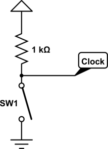
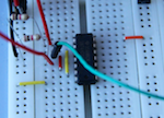
For testing purposes it's ok to generate the clock signal by hand. The easiest way to do this requires only a switch and a resistor configured like the figure on the right.
Let me just stop you right now and tell you that this won't work.
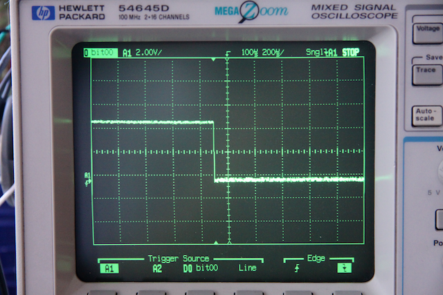
Why? Well, take a look at the output in an oscilloscope:
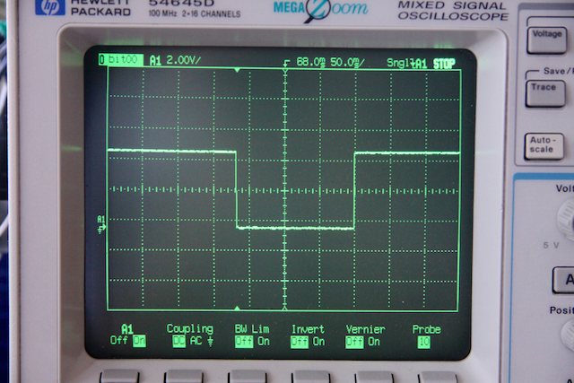
Doesn't look so bad, does it? Well, let's take a closer look at that falling edge to the left. Here it is, zoomed in about 250 times:
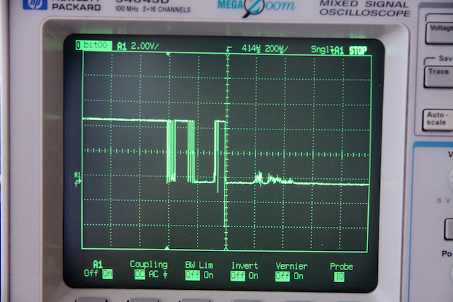
Now that's not pretty. If you used this clock circuit, for every time you press the button, the Z80 will receive a dozen pulses or two. That makes for some very unrepeatable behavior, and repeatability is what computers are all about.
A better clock signal
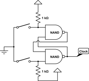
Here's a good clock generator. It requires two switches which are pushed alternately, two pull-up resistors and two NAND gates (e.g. 74HC00).
This is what's called an S-R-latch (S-R is short for Set-Reset).
Let's say the clock output is currently HIGH (+5V) and that no switches are pressed. The upper NAND gate then has two HIGH inputs, which means its output is LOW (0V). The lower NAND has one LOW input and one HIGH, which means its output is HIGH. By pushing the top button, one of the inputs to the top NAND is grounded so that its input is (LOW, HIGH) which means it outputs HIGH. This means the lower NAND gets the input (HIGH, HIGH) which makes its output LOW and when the button is released, the top NAND will have the input (HIGH, LOW) and thus still output HIGH.
It's a bit simpler to understand if you just think about it than if you try to read my messy explanation, but you must assume that the clock signal is either HIGH or LOW before you start thinking.
 Anyway, I built this circuit on a bread board and measured it the same
way as the last one.
Anyway, I built this circuit on a bread board and measured it the same
way as the last one.
Nice and clean. We've got our clock source.
Reset switch
When it comes to reset the Z80 is not as picky as with the clock signal. In fact, we can use the first attempt at a clock signal for reset.
The internal reset circuitry of the Z80 depends on the clock signal, so as long as the clock doesn't move, whatever happens with the reset signal doesn't matter.
This fact is important to rember for other reasons too; to perform a reset, the reset pin must be pulled low for a few clock cycles.
In other words: To perform a reset, push the reset button, toggle the clock a handful of times (minimum three), release the reset button.
That took me a while to figure out and is why you should always read your datasheets carefully, kids.
A similar note of caution: Don't leave the clock signal in its LOW state for any extended periods of time or the Z80 will forget its state. To be sure, always make the clock HIGH right after making it LOW. You could add an LED to show its current state.
Let's wire it up
Z80 tester
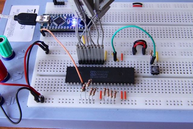
Here's a Z80 tester circuit wired up on my breadboard.
The connections are as follows:
D0-D7are pulled low through resistors of ~1kΩ./INT,/NMI,/WAITand/BUSRQare connected to +5V.+5VandGNDare connected as labeled./RESETis connected to a pull up resistor and a button as described above.CLKis connected to an Arduino nano which generates a 500 Hz square signal (I felt a bit lazy).A0-A7are connected to the logic probes of my oscilloscope.
But before I power this up, let's think about what we're expecting to see.
As we release the reset button (after keeping it down for three clock
cycles or more) the Z80 starts to read instructions at address 0x0000.
Since all data pins are permanently tied low it will read the value
0x00 which corresponds to a NOP instruction. This means it skips
ahead to address 0x0001 to read its next instruction and so on.
In other words, we expect the 8 lowest address lines to count upwards
binarily from 0 to 255. Since there are 8 address lines we're not
monitoring, it should make this count 255 times before getting back to
address 0x0000 again. But we won't be able to see the difference
between the counts.
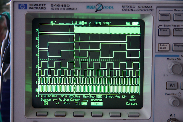
Ok, let's take a look.
 Just like that. This Z80 seems to be working fine.
All 255 addresses didn't quite fit in this picture, but you can see
address 0xXX00 to the left and 0xXX7B to the right.
Scrolling forwards a bit in time we find something interesting.
See that thing on A7? It's not stable, but is pulsing. The same
behavior can be seen on A8-A15. But why?
Dynamic memory refresh, that's why.
As I described in the last post; right after fetching an instruction,
the Z80 sends a refresh pulse to the memory chips. During this pulse, it
also sends an address on the 7 lowest address lines, i.e. A0-A6. The
other address lines are pulled low.
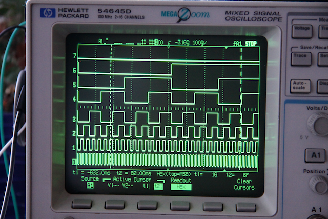
Let's take a closer look at the signals used.
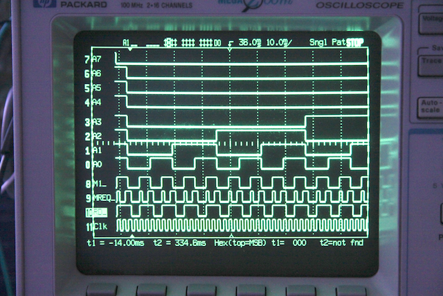
Here I also connected to the oscilloscope
/M1/MREQ/RDCLK
We can clearly see the instruction fetch cycle. /M1 goes low, followed
by /MREQ and then /RD. Then all three goes high while the processor
is decoding the instruction.
During the decode cycle, we see /MREQ go low again. This is the memory
refreshing. I didn't connect the /RFSH line to the oscilloscope but,
trust me, it goes low at about the same time.
Next is the execute cycle, which for the NOP instruction is nothing at
all, so the processor jumps right to the next instruction fetch cycle.
Ok... so the Z80 is indeed working as expected.
Next time we'll look at a control panel.